RISC-V GPGPU
Our 32-core RISC-V GPGPU, running on a real FPGA
- 2.38×faster than the ARM core on the same chip, for one n-body step
- 32RISC-V cores running in lockstep
- 1/17of the ARM core's clock speed
- 88%of the FPGA's logic (LUTs) in use
What it is
A small processor for parallel work, built from 32 RISC-V cores that all run the same instruction at the same time. The Zynq chip’s ARM core sends it a program and data, and it runs the work on all 32 cores at once.
We first ran it on a ZedBoard. It now also runs on the Smart Zynq SL, where my colleagues use it, and it is one of the two demos in my live FPGA lab.
Inside the GPGPU
A GPU gets its speed from running one program on many pieces of data at once. We built the same idea in Verilog, small enough to fit on one FPGA: 32 lanes that share everything they can, and copy only what each lane needs for its own data.
One front end for 32 lanes
Fetching and decoding an instruction 32 times would waste most of the chip. So there is one program counter and one decoder, and every lane gets the same decoded instruction in the same cycle. The lanes run in strict lockstep: when lane 0 takes a branch, the shared fetch follows it and flushes the instruction it had already fetched.
Each lane’s own pipeline
Behind the shared front end, every lane has its own registers and its own execute, memory and write-back stages, five stages in all. Register x31 holds the lane’s number, so the same instruction reads and writes different data on each lane.
- A forwarding unit passes a fresh result straight to the next instruction, without waiting for the register file.
- Multiplies run through a 3-stage pipeline built on the FPGA’s DSP blocks, so they don’t slow the clock.
- A hazard unit stalls the lane when an instruction needs a value that isn’t ready yet: a load, or a multiply still in its pipeline.
32 lanes, 2 memory ports
The block RAM that holds the data has only 2 ports, and all 32 lanes may want it in the same cycle. A crossbar picks two lanes each cycle, and the whole pipeline waits until every lane that asked has been served. If both picks write the same address, the second write is blocked, so memory never ends up half-written.
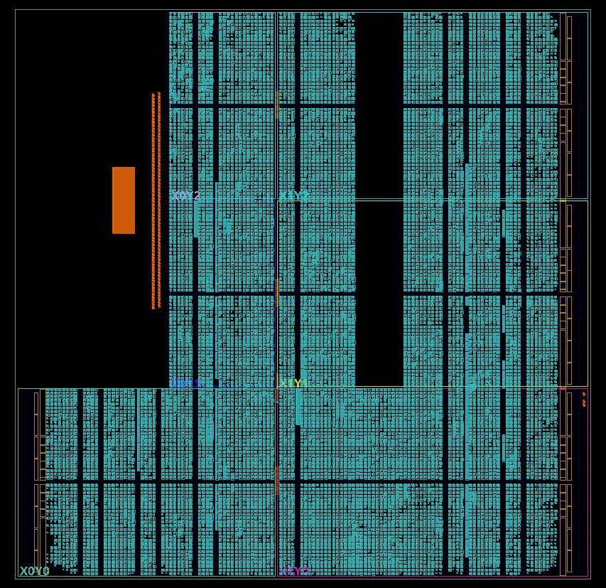
The whole design uses 88% of the FPGA’s logic.
From C code to the board
Compiling for 32 lanes
Each program is plain C, built twice: once as a bare-metal RISC-V kernel for the GPGPU, and once as a normal program on the computer, to compare results with. A small runtime starts every lane with its own 64-byte slice of stack, worked out from its lane number, so 32 copies of the same code never overwrite each other. The host writes a kernel’s arguments to a fixed spot in data memory before it starts.
Loading and running a kernel
The GPGPU moves through three phases: loading, running and dumping. While it loads, the host can write the program and the data. While it runs, the GPGPU owns the memories. When it finishes, the host reads the results back. A command processor accepts each host command only in the phase that allows it, so nothing can overwrite memory mid-run.
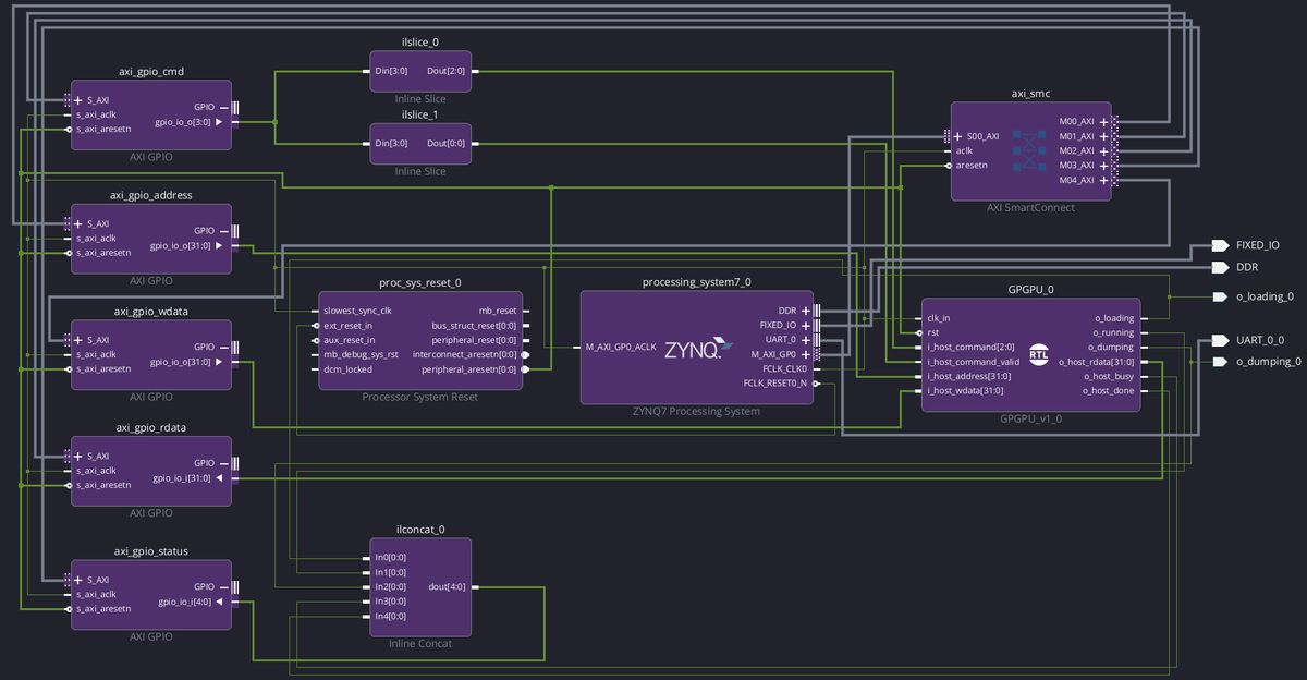
On the board, a small program on the Zynq’s ARM core receives commands from the computer over UART and turns them into reads and writes on AXI GPIO registers wired to the GPGPU. A first version put the UART inside the FPGA logic itself, but it proved unreliable, so we moved it to the ARM core. On the computer, a Python runner loads and runs each kernel, and a small adapter per program says what to send in and what to read back.
Verification
Checking every result
We wrote our own assembler for the test programs, and a model of the GPGPU in Python that predicts the exact state after every program. Every test compares the hardware’s registers and memory against it.
Programs that are safe to run in lockstep
Because all lanes share one instruction stream, a program has to keep them together. A checker runs each test program first and rejects it if it runs past 10,000 cycles, if two lanes would take a branch different ways, or if two lanes would write the same address in the same cycle.
Trying to break it
A fuzzer writes random programs aimed at the weak spots. Half the time an instruction reads the register the one before it just wrote, to stress forwarding. It also plants the hard cases on purpose: a load used straight away, a multiply followed by an instruction that needs its result, and back-to-back writes and reads to the same address.
On the real board
The same tests then ran end to end on the FPGA, through the same commands the host uses: load the program and data, run, read the memory back, and compare it with the expected output.
Results
One step of a 32-body n-body simulation, GPGPU at about 38.5 MHz against the ZedBoard's ARM Cortex-A9 at about 667 MHz.
That is 2.38× faster at about a seventeenth of the clock. Peak throughput is about 1.23 billion integer operations per second, and data memory moves 307 MB/s. The slowest part is the UART link to the host, at about 11.5 KB/s.
What’s next
We’re building version 2 with the same team. It adds graphics, DDR memory, branch divergence and warp scheduling.
- Done: Host controller over AXI
- Done: CLI for tests and synthesis
- Done: DDR memory controller
- Done: Graphics over HDMI
- In progress: Divergence, warp scheduling
- Next: Closer to 100 MHz
GPGPU v2
Our RISC-V GPGPU, now with DDR and HDMIIn progressWe're extending our RISC-V GPGPU from ECE338. It now reads and writes the board's DDR memory, grouping its lanes' accesses into bursts, and draws 1280×720 frames to an HDMI monitor, 60 a second. Next come branch divergence, warp scheduling and a clock closer to 100 MHz.Report, presentation and repository
Team


Tools
What this project was built with. Pick one to see where else I used it.